

| Product No.: | |
|---|---|
| Product Name: | Silicon Wafer |
Appearance
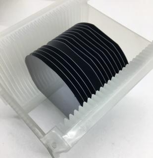
Silicon wafer is usually used for the thickness tooling of vacuum deposition system due to its superior flatness and reliable optical characteristics. Meanwhile, silicon wafer is a good substrate candidate for the fabrication of opto-electronic devices. Wafer cutting for suitable size is also available now.
Specification
|
Item |
Specification |
|
Orientation |
(100) +/-0.5deg. |
|
Type |
P-type doped by Boron |
|
Diameter |
100 mm |
|
Thickness |
525 +/- 25 um |
|
Resistivity |
1 ~ 100 ohm-cm |
|
Surface |
Single Side Polished |
|
Package |
25 pcs/pack |
|
Grade |
Test |
Application
1.Thickness tooling
2.Substrate for device fabrication
